waterkc said:
Well I am not sure how to upload images on the forum. I look around for a pic place or something and didn't see anything. I am dieing to send a pic of the layout I have so far. I ended up with 1 magnet on each also. Works like a charm.
any help on how to upload images would be great.
I can't wait until you post your pics so I can see how yours turned out.
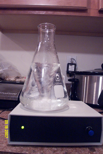
I ordered a 2" stir bar and a 2000ml Erlenmeyer last week, and they arrived
at about 5pm yesterday.
I have scavenged 7 hard drive magnets (one drive only had one), so I have
more than enough of those to get any size field that I want. I also have a ten
pack of rare earth magnets from Rockler Woodworking. They are 3/8" by 1/10".
I believe that I will use the hard drive magnets, but may change my mind yet.
The Rockler magnets are SUPPOSED to be for some refrigerator magnets for the wife.
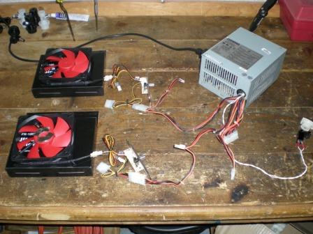
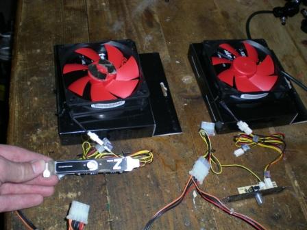
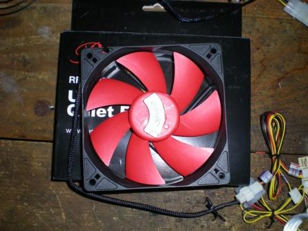
I have two standard 80mm case fans, and one 120mm case fan to play around with also.
I also scavenged the power supply from an old AT form factor computer
case, and am trying to use that. It appeared to be way too powerful, ramping
the fans up to full speed instantly, and sending that pig of a stir bar flying. I
pulled out an old fan speed regulator, and that seems to be helping some,
but I am still having some trouble. With one of the 80mm fans, I glued on a single hard drive
magnet, and it just does not seem to grab the bar well. With the other, I have two
magnets stacked together, and they seem to grab the bar better, but they also seem to
be slowing down the fan considerable, even causing it to not start spinning at times.
I would really like to try the 120mm fan, but it will need to have a large washer added to it,
as I have seen done in some of the other plans on here, as the inner workings of the fan itself
are keeping me from placing magnets where I would like to.
I just got done drilling a piece of Lexan, putting screws down through it, with
some spacers, and clamping the fan on underneath, with two hard drive
magnets stacked together and fairly well centered. I have not had a chance
to test it yet.
The advantage to the old AT power supply, assuming that it is truly not too
powerful, is that it already has the pin connectors for the fan, so there is no
extra work needed, you just plug it in and go. My fan controller can also handle
up to three fans, so ONCE I get this thing working right, I will probably expand
it to handle at least one more fan. I have two 6.5 gallon primaries, and five
5 gallon secondaries, so it would be nice to be able to run two batches of yeast
at the same time.
Well, we will see what tomorrow holds.
Hopefully I can get this thing working. I have a batch of cider that is just finishing
its first yeast, then I am going to pitch a champagne yeast into it to take it the
rest of the way, and I really want to test this thing out with that yeast.


![Craft A Brew - Safale BE-256 Yeast - Fermentis - Belgian Ale Dry Yeast - For Belgian & Strong Ales - Ingredients for Home Brewing - Beer Making Supplies - [3 Pack]](https://m.media-amazon.com/images/I/51bcKEwQmWL._SL500_.jpg)