You are using an out of date browser. It may not display this or other websites correctly.
You should upgrade or use an alternative browser.
You should upgrade or use an alternative browser.
Arduino-How to go from breadboard to finished product
- Thread starter Adeering
- Start date

Help Support Homebrew Talk - Beer, Wine, Mead, & Cider Brewing Discussion Forum:
This site may earn a commission from merchant affiliate
links, including eBay, Amazon, and others.
Are you going to etch your own board or have someone else do it for you?
I've been using http://fritzing.org/ to do my layouts. Haven't messed around with the PCB creator yet, but it seems to have some decent functionality at taking your breadboard wires and turning them into traces on a PCB
That's going to be tough with a mega. You have to etch a pcb to accept a surface mount atmega2560 chip. Those are only available in surface mount. Can you use a UNO instead? That's much simpler to make stand alone since there's a DIP form factor for atmega328. I proto'd a kegerator controller on an uno and transfered it onto a stripboard.
Adeering
Well-Known Member
No cant do it with a Uno, using the Mega ADK specifically for the android interface. Not looking to make a new board for the arduino, just wondering how to wire to the arduino more permanently.
This is my first time working with arduino for the most part, so finishing and how to make it a finished project I dont know. Havent worked with making PCB boards or anything either. So looking for some guidance on what others have done
This is my first time working with arduino for the most part, so finishing and how to make it a finished project I dont know. Havent worked with making PCB boards or anything either. So looking for some guidance on what others have done
I draw schematics and layout pcb with gEDA tool. with that you can etch your own or another option is the pcb group buy here: http://dorkbotpdx.org/wiki/pcb_order/
I buy a universal PCB and weld what a need on it, we actualy don't need a lot a stuff, for now I got 3-4 resitor and a lot a power/neutral going to sensor and lcd and ssr.
I'll put everything in a box with some switch and connectors.
I 'll post pic once over.
I'll put everything in a box with some switch and connectors.
I 'll post pic once over.
I am just exploring this myself.
Have you seen the blank shields for the Arduino. You wire and solder them yourself, then set them on top of the arduino mega? For example, http://www.adafruit.com/products/187 or http://dangerousprototypes.com/2011/01/09/arduino-shield-database/ And get some hex nut screws and nuts, at the corners of the boards, to make the connections more permanent. Also, check this out: http://www.arduino.cc/playground/Learning/Tutorials
Have you seen the blank shields for the Arduino. You wire and solder them yourself, then set them on top of the arduino mega? For example, http://www.adafruit.com/products/187 or http://dangerousprototypes.com/2011/01/09/arduino-shield-database/ And get some hex nut screws and nuts, at the corners of the boards, to make the connections more permanent. Also, check this out: http://www.arduino.cc/playground/Learning/Tutorials
Adeering
Well-Known Member
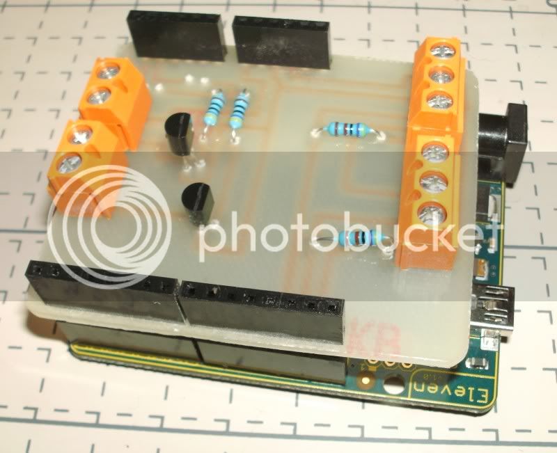
I ended up going with the prototyping wingshield from adafruit. It makes for easy connection to the pins and nice little board to solder on the needed resistors and pots. Gonna put everyting into a small plastic box and then mount that in my panel.
chuckjaxfl
Well-Known Member
I've recently started this part of the hobby.
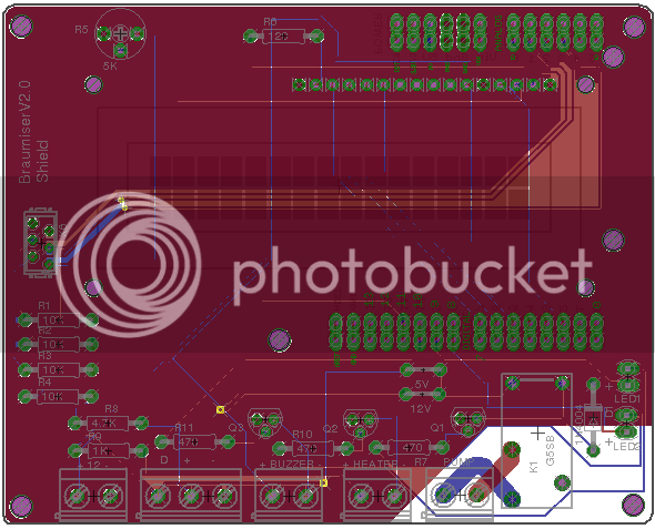
The route I've taken is to learn Eagle. It's not intuitive, but it's powerful. Plus, the reference files on the Arduino site are in Eagle. For my shield, I downloaded the UNO reference file and deleted everything except the outline, the stackable headers, the ICSP header, the reset, and I left the USB connector outline and moved it to the "keep out" layer. So, now I have a "starter" schematic and pcb layout for shields, like this. This seemed an easy way to me to line everything up, especially that weird 0.016 space on the digital side.


The route I've taken is to learn Eagle. It's not intuitive, but it's powerful. Plus, the reference files on the Arduino site are in Eagle. For my shield, I downloaded the UNO reference file and deleted everything except the outline, the stackable headers, the ICSP header, the reset, and I left the USB connector outline and moved it to the "keep out" layer. So, now I have a "starter" schematic and pcb layout for shields, like this. This seemed an easy way to me to line everything up, especially that weird 0.016 space on the digital side.
chuckjaxfl
Well-Known Member
This is a shield I made to use the UNO as a programmer. I can put 8/168/328's in one of the ZIF sockets. The other is setup to program attiny84's at one end, attiny85's at the other, and I have a six pin header one there as well.
I sent the Gerber files (made w/ Eagle) to BatchPCB for that one. I paid for one, they sent two. I understand this is not rare, that they will make/send duplicates to fill a board more quickly.
The other pic is a little PWM I drew, also in Eagle. This one I sent to iTead. Cheaper per board, they may have been a little quicker, too. They make them in lots of ten, though. Still, I paid $18 for 10 little boards, and I think almost the same pice for two shields.
Adeering,
Might want to have a look at the thread about wire wrap or point to point. This is a discussion pointed directly at what options are available to move from a proto board to reality with out burning a PCB. So far I have decided to go woth pogo pins and wire wrap. It is very similar to telephone switching office wiring technique. If you need info on the parts you will need and the tool gimme a holla.
Wheelchair Bob
Hey guys,
Wanted to throw some Of my knowledge into the wind and see if it'd help you out.
Eagle is a great PCB tool that's free. I have some technicians that use it to fab their own startup boards.
I/we use cadence orcad and allegro at my office. It's expensive, but there's a great book out there that's written towards using cadence but includes a wealth of pcb manufacturing/design knowledge. When I was doing my own boards for a smaller company I learned to love this book. It by kraig mitzner and it's called "complete pcb design with orcad and pcb layout" or something similar.
If you order 1 pcb, chances are that you'll get multiples because you might have paid for multiples...or you found yourself a really cool board house.
PCB material (typically called FR4, although there are others depending in your application) is cut to standard sizes. When you submit your gerber files to a board house, they try to utilize an entire panel to minimize manufacturing costs. Typically you'll pay for the whole panel regardless if you use the whole panel or not, so next time ask them how many of your design they can fit into a standard panel and quote that. Some sites like pcbexpress may fit a bunch of random designs into a panel before they run the batch.
If you order 1 pcb, chances are it'll be a very expensive pcb. Try quoting 5 or 10 and you'll see very little cost increase, yet your per board cost should drop significantly. Always order multiples. If you buy only 1 and then happen to fry a trace, it's expensive to replace. If you order 2+ and fry a trace, you already have extras to keep moving with.
Also look at the manufacturing constraints of the boardshop. I know advanced PCB has them on their website, but when you ship a design in, they'll run a DFM (design for manufacturability) on your design and either tweak it or come back to you with the issues. Simple stuff typically, like improper drill sizes, spacing constraints, not enough copper, etc.
Hope that helps a bit and good luck with your project!
-scott
chuckjaxfl
Well-Known Member
I ended up going with the prototyping wingshield from adafruit. It makes for easy connection to the pins and nice little board to solder on the needed resistors and pots. Gonna put everyting into a small plastic box and then mount that in my panel.
Where are you with this? Have you got anything to show yet?
I/we use cadence orcad and allegro at my office. It's expensive, but there's a great book out there that's written towards using cadence but includes a wealth of pcb manufacturing/design knowledge.
What do Orcad & Allegro that Eagle doesn't?
I'm aware of the freeware version of Eagle's obvious limitations of 2 layers and maximum size. But the sum of my experience is pretty much wrapped up in this thread, plus a number of other tiny home-etched projects. I wouldn't know what I was paying for, or what even to look for in PCB software. I did some drawings with pcbExpress. It's not even a real tool compared to Eagle. Is there a similar difference between Eagle & the two packages you mentioned?
Chuck, my apologies if I maybe caused confusion.
Cadence is orcad's schematic package. Allegro is there fancy layout package.
Probably the largest difference between orcad and eagle is the cost of the full package which includes a bunch of features that for the most part I dot use...with exception to spice - a circuit simulator. I think there is a student or trial version of the schematic layout program...but you're limited to 30-40 components.
I think a used copy of mitzner's book is still a good reference for pcb layout theory and design guidelines.
The inability to do more than 2 layers in eagle is a downer, I didn't know that!
I imagine I'll do a board with 4 layers when I get around to my automated brewing setup, so this is good to know. Although if you have the space, 2 layers will be completely adequate.
Another thug to consider in your design, if you end up having power (high current) traces on your board, you'll want to ensure you have enough copper to keep your losses minimal otherwise theres a risk of fire (worst case) or burning up a trace (more likely). There's some calculators on the web that can help with this math too. If you don't have any high current stuff, then your probably cool!
I don't know if anyone has suggested Sparkfun, but I work next door to these guys and they're super-huge on the arduino front. They are also big on using eagle for hobbiests. Here's a link to some of their tutorials on eagle and stuff:
http://www.sparkfun.com/tutorials/category/1
Appologies if I missed something; my home Internet is down so Ive been surfing/replying through the iPhone app.
-scott
matho
Active Member
I have used eagle demo to make up a PCB and also an open source program called Kicad, eagle is great as there is a huge library of parts but I did find that I still had to modify a couple of footprints for what I wanted to do. Kicad is a good open source program but as with eagle it takes time to learn and the libraries are limited. Both programs can be printed to PDF which is great if you want to etch your own boards. I used the laser printer on glossy method for small one off PCBs
how I make my own PCB's
http://www.mediafire.com/view/?j43whn9tt446p73
just make sure you have an etch resistant pen to do small touch ups.
I also got PCB's made up by a factory, I used this place in china
http://www.seeedstudio.com/depot/fusion-pcb-service-p-835.html?cPath=185
not bad service but it takes about 3 - 4 weeks to get boards
cheers steve
chuckjaxfl
Well-Known Member
with exception to spice - a circuit simulator
Which does what? You mean it actually, uhm.. virtually... breadboards whatever you draw? You can adjust pots and watch the voltage divide and such?
The inability to do more than 2 layers in eagle is a downer, I didn't know that!
The freeware version limits to 2, yes.
I don't know if anyone has suggested Sparkfun,
Yup, what little I know, I learned from Sparkfun, LadyAda, and Jeremy Blum tutorials.
I also got PCB's made up by a factory, I used this place in china
http://www.seeedstudio.com/depot/fusion-pcb-service-p-835.html?cPath=185
not bad service but it takes about 3 - 4 weeks to get boards
I think, but don't know for sure, that seeedstudio and iTead are separate divisions of the same company. My experience with them matches yours.
I don't think batchPCB was any quicker, but they're pretty forthcoming about the turnaround time.
Not trying to hijack the OP, cause I believe this is part of the planning process, I'm trying to determine how many of these boards will be needed off the Arduino? I started by looking over Emile's Home Brewing Web site, specifically the hardware page at http://www.vandelogt.nl/htm/hardware_uk.htm. I notice he made several "interface circuit" electronic boards:
1. for pressure sensors;
2. for modulating gas valve;
3. for heating and pumping elements;
4. for valves; and
5. for PC Interface.
I expect a little bit of this, but how much of this is really needed with the Arduino. Can I purchase products that do not need this electronics or have the electronics built in? For example, I seriously believe I can eliminate the PC Interface and use a USB interface with Processing on the PC side.
EDIT: I realize this is hard to answer, but can we assume (for now) that I would like to do the same thing as Emile, but with an Arduino replacing his microprocessor. thanks...
Thanks,
I use PADs layout from mentor graphics at work but like orcad and allegro it is probably out of the price range for the average hobbyist. But with that being said you can use it in demo mode without a license and layout a smaller board and still be able to save the project and export the gerber files. I'm not sure what the cutoff is but I think it is a certain number of nets. It is a very powerful tool and is very commonly used in the industry.
I used PCBexpress in college and found it to be a PIA.
Advanced circuits is good for fast turn around times but can be rather expensive. I just sent out a 4 layer board that is 3x5 inches tonight and it is going to cost us $1800 to get 15 boards fabbed on a 1 day turn. We only needed 5 PCBs but there wasn't much price difference between 5 and 15. We have only used them for fast turn arounds so I am not sure how cheap you can get down to with just a 2 layer board and a slow turn around time. You can also reduce costs by getting your design to meet their standard package with things like no plated slots or tight corners on board cutouts. They do a good job of checking over your design for any issues before they make it and they also have a free DFM (design for manufacturing) tool to also help catch any potential issues.
I have never tried the etching process but PADs will also let you print your gerber files to scale so you could use that for etching. I use that feature to verify footprints of new parts by printing out the footprint and placing the part on the piece of paper to make sure it is the right size and all the pads or though holes are in the correct location.
I also noticed yesterday when I was on advanced circuits site that they have a free layout tool and it doesn't sound like it has any limitations to it. Might be worth giving that a try. It has a huge library of parts so hopefully you can get away without having to create any new decals.
"I also noticed yesterday when I was on advanced circuits site" ^^^
Got a link to that site?
WCB
I think it's this one: http://www.4pcb.com/free-pcb-layout-software/index.html
helibrewer said:I think it's this one: http://www.4pcb.com/free-pcb-layout-software/index.html
Yup that's it. If anyone here gives it a try let me know how you like it or better yet how it compares to any of the other free tools out there. I may have to start using it if I get a new job and am no longer doing any PCB layout in my new position.
Yup that's it. If anyone here gives it a try let me know how you like it or better yet how it compares to any of the other free tools out there. I may have to start using it if I get a new job and am no longer doing any PCB layout in my new position.
"Linux and MAC OS are not currently supported."

I go back and forth between Eagle and DipTrace. DipTrace has much better tools for creating new components and especially solder pad layouts. I usually end up editing the xml file in Eagle when I create new layouts -- a PITA. Both of them have free versions for home use with limitations I have yet to encounter. The 3D viewing tool in DipTrace is very nice for visualizing and inspecting a board, although eagle is supposed to have a tool now also (and I'm a big fan of SketchUp).
As far as getting PCBs made goes -- we have a local source that batches boards together for $5/sq in for 3 copies. They have fantastic quality and good specs (6 mil traces...). They also do 4 layer boards.
As far as getting PCBs made goes -- we have a local source that batches boards together for $5/sq in for 3 copies. They have fantastic quality and good specs (6 mil traces...). They also do 4 layer boards.
Similar threads
- Replies
- 19
- Views
- 619
